|
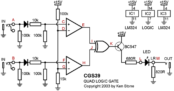
The Quad Logic Gate is a very simple module that can be built in one of five flavors : XOR, OR, AND, NOR and NAND. It is a simple way to gain additional control of gate and trigger pulses within a system. It can also be used for some simple signal multiplying. The XOR is well known as a square wave "ring modulator", though interesting effects can also be generated using the other configurations. Each gate has an in-built LED to indicate the status of the output of that gate. With some chip types, it is also possible to have some of the gates presented on the panel as basic inverters. For XOR and NOR gates, tie the disused input of that gate to 0V. For NAND gates, tie the disused input of that gate to +15V. It is not possible to create inverters with AND and OR gates. A little on how it works:

The schematic of the Quad Logic Gate.
Connection/pin identification table for the above diagram. Note that there are two LM324 chips involved, one for In 1 and 2, the other for In 3 and 4.
Each input is configured to detect a voltage over approx. 2 volts. When this voltage is reached, a logic HIGH is presented to the corresponding gate input. The output will react to what is present at the inputs, and the result, depending on the gate chip used, is buffered by the emitter follower, and used to drive the LED and output jack.
Construction

The component overlay. Note that this version of the board (the prototype run) incorrectly connects to the negative rail. The ferrite bead on the negative rail should be omitted (marked in red), and a link used instead of the corresponding capacitor (marked in blue). Use LM324, not TL074 as marked.
Before you start assembly, check the board for etching faults. Look for any shorts between tracks, or open circuits due to over etching. Take this opportunity to sand the edges of the board if needed, removing any splinters or rough edges. When you are happy with the printed circuit board, construction can proceed as normal, starting with the resistors first, followed by the IC socket if used, then moving onto the taller components. Take particular care with the orientation of the polarized components such as electrolytics, diodes, transistors and ICs. When inserting ICs into sockets, take care not to accidentally bend any of the pins under the chip. Also, make sure the notch on the chip is aligned with the notch marked on the PCB overlay. In this case I recommend using a socket for the CMOS chip, as this will allow different chips to be substituted for the purpose of experimentation. Valid choices are:
There are four LED return pads, marked LR1-4. The order in which these are used is not critical. Each pair of inputs to a gate share the same designator. The order in which each pair is wired to the panel sockets is not critical. Notes:
Parts list This is a guide only. Parts needed will vary with individual constructor's needs. If anyone is interested in buying these boards, please check the PCBs for Sale page to see if I have any in stock.
Can't find the parts? See the parts FAQ to see if I've already answered the question. Also see the CGS Synth discussion group.
Article, art & design copyright 2001 by Ken Stone
| ||||||||||||||||||||||||||||||||||||||||||||||||||||||||||||||||||||||||||||||||||||||||||||||||||||||||||||||||||||||||||||||||||||||||||||||||||||||||||||||||||||||||||||||||||||||||||||||||||||||||||||||||||||

