|
The CV Adapter is an addition to the Gate Sequencer converting it to a traditional eight-step control voltage sequencer. It simply adds a single channel no-nonsense 8 step analog output. Additional boards can be added to increase the number of channels as desired. The pots are assigned to a particular step during construction, so the board can be mounted either vertically or horizontally as required. All clocking, sequence length and reset functions etc. are handled by the main gate sequencer board. A little on how it works:

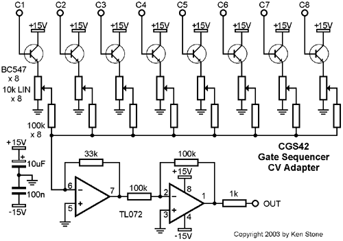
The schematic of the core of the CV Adapter.
To avoid overloading them, each of the column drives from the Gate Sequencer is buffered by a general purpose NPN transistor such as a BC547 or 2N3904 wired as an emitter follower. The buffered column drives are used to apply a voltage across each of the pots in sequence. The wiper of each pot picks up the reduced voltage, which is then fed into a non-inverting mixer based around a dual op-amp. As only one put has a voltage across it at any time, only one voltage is fed into the mixer. The remaining inputs are all at 0 volts, and as such have no effect on the summed output. This board could of course be connected to other signal sources if desired, or even used as a small mixer, if the transistors were omitted and the input signals were fed directly into the pots.
Construction

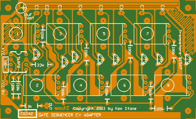
The component overlay. Connections can be determined from the circuit diagram. Before you start assembly, check the board for etching faults. Look for any shorts between tracks, or open circuits due to over etching. Take this opportunity to sand the edges of the board if needed, removing any splinters or rough edges. (Note that on the first run of PCBs a corner hole is missing. I don't know why - it was on the artwork.) When you are happy with the printed circuit board, construction can proceed as normal, starting with the resistors first, followed by the IC socket if used, then moving onto the taller components. Take particular care with the orientation of the polarized components such as electrolytics, diodes, transistors and ICs. When inserting ICs into sockets, take care not to accidentally bend any of the pins under the chip. Also, make sure the notch on the chip is aligned with the notch marked on the PCB overlay. The order the pots will be sequenced is indicated by a small number in the middle of the overlay for each pot. It follows left to right, with no consideration for the vertical offset. This way, each gate sequencer column can be represented by a vertical line. If you would prefer a different arrangement, the wires connecting the "C" pads on this board to the main gate sequencer can be shuffled as required. There is no power input jack on this board, as it is designed to be jumpered directly to the host gate sequencer board. You will find you need to run a negative feed to the gate sequencer board if oneis not already present.

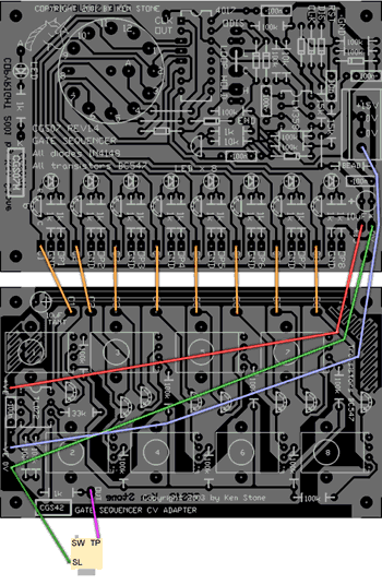
An example of hard wiring the CV Adapter to the gate sequencer board. Notes:
Parts list This is a guide only. Parts needed will vary with individual constructor's needs. If anyone is interested in buying these boards, please check the PCBs for Sale page to see if I have any in stock.
Can't find the parts? See the parts FAQ to see if I've already answered the question. Also see the CGS Synth discussion group.
Article, art & design copyright 2001 by Ken Stone
| ||||||||||||||||||||||||||||||