Gate Sequencer for music synthesizers. Obsolete. See the CGS89 Gate Sequencer. See the CGS Synth discussion group, and notes below for modifications suggested for this unit. Later runs of PCBs differ slightly from these. Following a number of requests, I've produced a set circuit boards for this project. At the same time, the circuit underwent some upgrades, including making it cascadable. On top of that, one of the circuit boards makes a worthwhile module on its own. Again I have chosen the "construction kit" approach for this project. There is more than one way to assemble it, depending on available parts or needs. SPDT switches can be used to make a basic but adequate gate sequencer. SPDT Center Off switches can be used instead to produce something with 1/2 step resolution assuming a square wave clock is used. Note that these 1/2 steps are fixed at the beginning of each step cycle. See the timing diagrams below for an example. A new expansion board has also been added, the Gate Sequencer CV Adapter, which allows this to be adapted into a regular eight-step sequencer. How to use this module: By itself, the main board of the gate sequencer can be used as a sequential pulse generator. When clocked by an external source, each of its outputs will come on one after the other. This can be used to sequentially trigger up to eight events. An example would be to set the number of steps to 2, then connect outputs 1 and 2 to two drum sound generators. A pulse train fed to the clock input would then produce a drum roll alternating between the two drum sounds. When coupled with the switch bank and buffer boards, rhythms of up to eight steps can be created. Each switch bank and buffer board contains two channels. Additional switch bank and buffer boards can be connected to main board to produce gate sequencers with more channels. While these outputs can be used to trigger drum sounds, that is not their only use. They can be used to trigger envelope generators, step waves in wave tables, drive other sequencers etc. Once you have a gate sequencer in your modular, you will wonder how you ever survived without it. Multiple gate sequencers can also cascaded for longer rhythm lengths, or more channels. To cascade the outputs of several units, simply connect the "Full Out/Mix Out" and "Pulse Out" outputs on the first unit to the corresponding Cascade inputs on the second unit and so on. Alternately, simply run all corresponding Cascade inputs to a multiple jack. The output buffers are designed in so they can be wire ORed simply by connecting them together. Experiment with it. A little on how it works: First we will consider the main board.
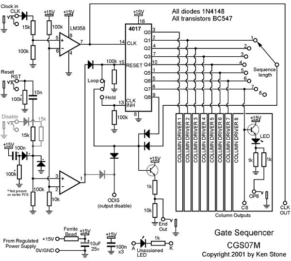
The schematic of the main board of the Gate Sequencer. Grey components may not be on all versions of the PCB. They show (more or less) the original Disable input circuitry. Both halves of an LM358 op-amp are used to shape the input signals. These take whatever signal is fed into the module and convert them to signals appropriate for driving the rest of the circuitry. With the values given, the sensitivity is set at around 2V, allowing triggering from signals with a +/- 10 volt swing, or with a 0V to +10 volt swing, both of which are common in modular synths. The output waveforms of some modules will never fall below the 1.4V level, preventing triggering. This can be solved by increasing the value of the 10k resistor between pin 6 of IC1 and ground to 22k. The input could also be capacitively coupled if need be. The clock signal is used to step the 4017 decade counter through its steps. The sequence length switch is used to select at which step the counter will stop or be reset. When the Loop/Hold switch is set to "Loop", the counter will be reset when the selected terminal count is reached and the counter will continue to count from "0". There will also be a very brief pulse at the "End Out" output jack. When the Loop/Hold switch is set to "Hold", the counter clock input will be disabled at the selected terminal count and will not continue until a reset pulse is received, the Loop/Hold switch is returned to "Loop", or in some circumstances, the number of steps selected is changed. When the selected terminal count is reached, there will also be a constant logic HIGH (approx. 13V) at the "End Out" output jack. This signal can be fed to the "Reset" of the following cascaded Gate Sequencer, if used. A positive voltage of sufficient magnitude applied to the "Reset" input will reset the 4017 counter, but allow it to continue counting. Each of the first eight outputs of the 4017 are buffered with a transistor wired as an emitter follower. Any general purpose NPN transistor will work here. I use the BC547 because it is the most common transistor in Australia. This buffer drives an LED to display which step is active, as well as the individual outputs for each step. The following outputs are for internal use only, when connected to the switch bank and output buffer boards: ODIS (output disable), CLK OUT (clock out), C1 to C8 (column outputs). Do NOT bring these output out to front panel jacks, as you may damage the circuitry.
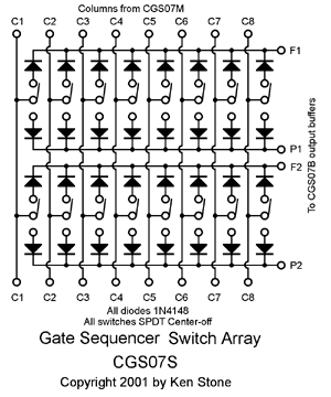
The schematic of the switch matrix of the Gate Sequencer. The switch matrix as show in the schematic, assumes that SPDT Center-off switches have been used. The column inputs C1 to C8 are taken HIGH sequentially by the 4017 on the main board. At any given time, only one column will be at logic HIGH. The remainder will be logic LOW. Let's consider the top left switch. When C1 goes HIGH, depending on the position of the switch, a HIGH will be transferred through to either F1 or P1, or blocked if the switch is in the center-off position. When any other column is HIGH, the diodes on this switch prevent it from having any effect. The channel outputs F1 (full step length for channel 1) and P1 (partial step length for channel 1) are then fed to the buffer board for processing.
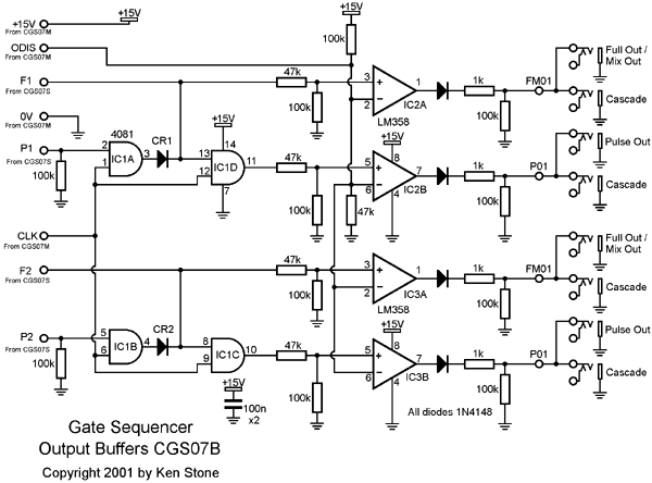
The schematic of the buffer board of the Gate Sequencer. The buffer board is designed in such a way as to be able to process modules that are made using either ordinary SPDT switches, or the center-off variety. The latter are much more versatile, but not essential. First, let us consider any of the switches for a given channel are set to "full". This is the position shown on the schematics, and corresponds to the levers on the switches being in the down position. This will result in a pulse train of HIGHs being present on the F1 input of the buffer board. Each pulse in this train corresponds to the full period of the clock signal. When two consecutive switches are on, this results in a HIGH pulse that is a full two clock cycles long. When three consecutive switches are on, this results in a pulse that is a full three clock cycles long and so on. Assuming there is no voltage present on the ODIS input, these HIGHs are sufficient to send the output of the corresponding output comparators HIGH resulting in a HIGH of around 13 volts at the "Full Out/Mix Out" output. This output is good for driving envelope generators when note lengths of two or more clock periods are required. At the same time this is happening, these HIGHs are also being AND gated with the clock signal resulting in a train of pulses that are of equal length to the HIGH portion of the clock signal. When two consecutive switches are on, this results in two consecutive HIGH pulses each that is equal length to the HIGH portion of the clock signal. These are processed by an identical buffer/comparator and fed to the "Pulse Out" output. This output is good for driving envelope generators or percussive events when a pulse per selected note is required. This is the output most likely to be used if you are using the module to make simple drum tracks. The above also describes the functionality available when ordinary SPDT switches are used. Now, let us consider center-off switches are being used, and any of the switches for a given channel are set to "pulse". This corresponds to the levers on the switches being in the up position. This will result in a pulse train of HIGHs being present on the P1 input of the buffer board. These HIGHs are also being AND gated with the clock signal resulting in a train of pulses that are of equal length to the HIGH portion of the clock signal. These HIGHs are then OR gated (via the diode) with the train of pulses coming from any switches that are set to the Full position. This will result in mix of full period and partial period signals being present at the "Full Out/Mix Out" output. These partial pulses are also present at "Pulse Out" output.
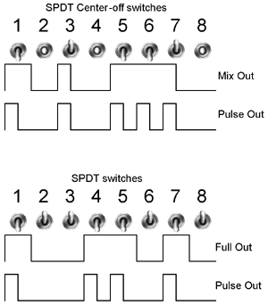
Two timing examples from the Gate Sequencer. This assumes the clock signal has a 50% mark/space ratio. The top row demonstrates the possibilities when using SPDT Center-off switches, while the bottom row demonstrates the possibilities when using ordinary SPDT switches.
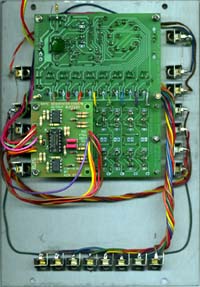
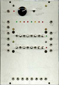
ConstructionOkay, so my module as pictured above doesn't look as inspiring as a lot of my other modules. While it is electrically complete, I have left it in this unfinished state pending the addition of either a second bank of switches or the new preset module I am working on. I have the inputs for Clock, Reset and the cascade inputs to the left, while the Event End, and the bank outputs are to the right. For convenience, I have run put a second clock jack to the right of the module, wired directly to the clock input jack, allowing easy cascading of the clock signal. Along the bottom are the eight individual step outputs. I have used four different colored LEDs for the steps, with beats 1 and 5 in green, 2 and 6 in yellow, 3 and 7 in orange and 4 and 8 in red. This helps give a quick visual indication of what step the sequence is up to. The LED near the rotary switch and the two LEDs near the outputs of the switch bank are currently not wired to anything. My panel is three Moog panel widths wide. I imagine it could be squeezed into three MOTM panel widths without much trouble.
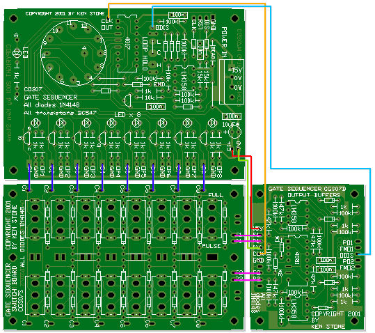
The component overlays and interconnection of the PCBs. Not show here are power connections and connections to input and output jacks. These can be determined from the circuit diagram. Before you start assembly, check the board for etching faults. Look for any shorts between tracks, or open circuits due to over etching. Take this opportunity to sand the edges of the board if needed, removing any splinters or rough edges. When you are happy with the printed circuit board, construction can proceed as normal, starting with the diodes and resistors first, followed by the IC sockets if used, then moving onto the taller components. Take particular care with the orientation of the polarized components, the diodes, LEDs, electrolytics and the transistors and ICs. You may want to leave soldering in the LEDs until you work out what height they will need to be to pass through holes in the panel. When inserting the ICs in their sockets, take care not to accidentally bend any of the pins under the chip. Also, make sure the notch on the chip is aligned with the notch marked on the PCB overlay. Please note that the CMOS chips are static sensitive devices, so make sure you handle them correctly. On the schematic I have ghosted in the approximate circuit of the original "Disable" input for those who have an older board, or still wish to included it. Sending a HIGH gate signal to it will reset the counter, and disable the outputs. There are three modifications needed if you are using one of the first run of PCBs:
There are two modifications needed if you are using one of the second run of PCBs:
There are other differences between the first and later runs of the PCB, such as the omission of the Disable input, which proved to be useless as it was. If you wish to use a MOTM style power connector, you will either need to use a 90° connector or to mount it on flying leads. There is insufficient space between the PCB and the panel for a regular connector to fit. When mounting these boards on the front panel, you will find that the height of the switches and the thickness of the panel material will determine the required gap. The main and switch boards will both need to be mounted firmly to the panel to limit flexing. I've used 15mm spacers with a 2mm deep nut on top, giving a total of 17mm on a panel that is around 1.4mm thick. The rotary switch is not secured to the panel and the other switches are a little recessed. The Rev 1.4 PCBs can be built as is, unmodified, except for the LM358 being replaced with a TL072 if needed. Also there is a 100n between pins 1 and 3 of the LM358/TL072 that can be omitted, especially if you are having problems with the reset function. See the notes below.
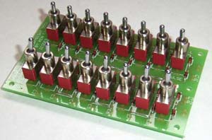
The switch board. The buffer boards can be mounted on brackets elsewhere, so as not to waste panel real-estate. Mine is mounted further up the same bolts that are holding the switch board. If using multiple switch banks, space your PCBs evenly so there will be no differences in the distance between channels. Allow 0.1 inch gap between switch bank PCBs to achieve this. Also on the switch board are numerous unassigned holes. These are for LEDs to indicate both channel output, and which column is active, though there is NO driver circuitry supplied. They are simply provided as a courtesy so more advanced experimenters can use them if they wish. The boards have been designed to take a variety of C&K switches, to allow for surplus switches to be used if found. I have used C&K 7103, which at first look are quite unsuitable, being 90° PCB mount. The brass pins were straightened, and the over-long white plastic portion of the toggles were shortened by about 1/2 inch. If you are in Australia, Jaycar has these at $1.05 for 10 to 24 units or $0.95 for 25 and over. The part number is ST-0564. As the PCBs are no longer being produced, I am presenting the artwork here for those that wish to home etch. The art is done at 300dpi, even though .gif format saves them with the incorrect value of 72 dpi. Right-click to save. Boards may be produced for yourself, or for friends, but NOT made available for public sale. If you produce a run of boards as a group project, extra boards may be sold via synth forums. Note that I will not provide technical support for boards that have not been supplied by me.I suggest you ask on one of the CGS support forums if you have trouble. Buffer overlay
Preset board
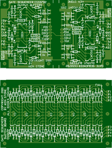
The preset boards for the gate sequencer. The preset board for the gate sequencer is simply a more compact version of the switch bank. Instead of toggle switches, DIP switches have been used, allowing a much greater concentration of switches in the area. Each DIP switch corresponds to a column, and contains switches for eight rows. It can be wired so that pairs of rows control full and pulse outputs instead of single center-off switches, giving a total of four channels per preset board. Alternately all switches could be used for either pulse or full, resulting in eight channels, though if you do this, you will need to obtain an extra pair of buffer boards. As can be seen from the image, the buffer boards have been joined into a common board. They are identical to the single board and can be separated if needed. Two traces, GND and ODIS have been connected. All others will need to be wired. The 100k and 47k resistors connected to the non-inverting input of the comparators should only be used on one buffer board. All other buffer boards share these resistors via the ODIS line. Column connections to the preset switch board are on the copper side of the board, under each DIP switch. Make sure you install all the DIP switches facing the same direction!
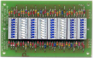
The preset board. I've used salvaged diodes. These dip switches came with protective plastic across the top, hiding the color of the switches, and leaving a sticky mess when removed. More Photos: Notes:
Parts list (excludes preset board and buffers) This is a guide only. Parts needed will vary with individual constructor's needs. If anyone is interested in buying a set of these boards, they are available as sets of three (main, switch and buffer, or preset board and two buffers). Check the PCBs for Sale page to see if I have any in stock. Due to the small number of boards produced this run I am only selling them as complete sets. If you wish to have a four channel gate sequencer, you will have to purchase two sets. Consider using the spare main board as a sequential pulse generator.
Can't find the parts? See the parts FAQ to see if I've already answered the question. Also see the CGS Synth discussion group.
Article, art & design copyright 2001 by Ken Stone
| ||||||||||||||||||||||||||||||||||||||||||||||||||||||||||||||||